🧪 General · 3 January 2018
What is Graphene?
In 2004, two physicists at the University of Manchester performed what may be the most understated Nobel Prize-winning experiment in history: they pressed a piece of sticky tape against a lump of graphite, peeled it off, and examined the thin layers left behind. By repeating this process — pressing, peeling, successively thinning — Andre Geim and Konstantin Novoselov isolated a single atomic layer of carbon atoms for the first time.
They called it graphene, and the world's materials scientists immediately began describing it as the most remarkable material ever discovered.

What Graphene Is
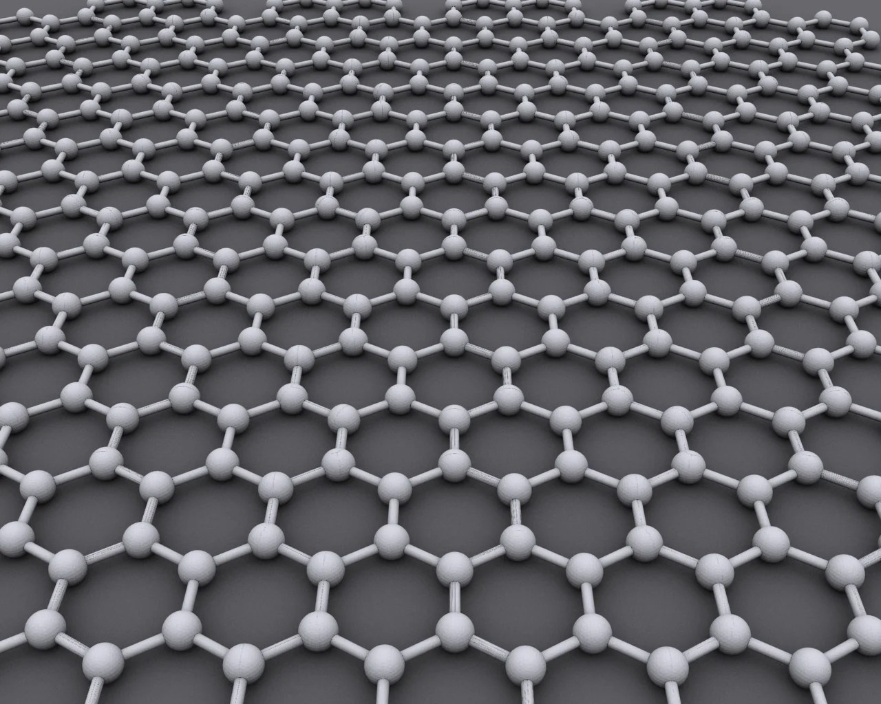
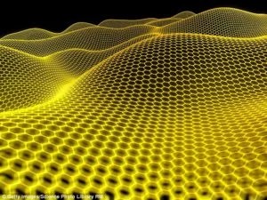
Graphene is a single layer of carbon atoms arranged in a flat hexagonal lattice — a honeycomb pattern with one atom at each vertex. It is exactly one atom thick: 0.335 nanometers, a dimension so small that it takes roughly 200,000 graphene layers stacked on top of each other to match the thickness of a human hair.
Graphene is simply what graphite is made of. When you write with a pencil, you deposit thin layers of graphite on paper — and there is a genuine possibility that some of those layers are graphene. The difference is that until 2004, no one had managed to isolate a single layer and study it systematically.
The hexagonal structure arises from carbon's chemistry: each carbon atom in graphene forms three σ bonds with its three nearest neighbors via hybrid orbitals. These are among the strongest chemical bonds known. The fourth valence electron from each carbon occupies a π orbital perpendicular to the plane, and these π electrons are delocalized: they are not bound to any particular atom but are free to move throughout the entire sheet.
Why It's Extraordinary
Mechanical Strength
Graphene is the strongest material ever measured. In 2008, Columbia University researchers pressed a diamond-tipped probe into a suspended graphene membrane and measured its elastic properties. Result:
For comparison, stainless steel has a tensile strength of about 860 MPa — graphene is roughly 150 times stronger. In vivid terms: it would take an elephant standing on a pencil tip to pierce a sheet of graphene the thickness of kitchen cling wrap.
| Material | Tensile Strength | Notes |
|---|---|---|
| Stainless steel | 860 MPa | Structural metal |
| Kevlar | 3,620 MPa | Body armor |
| Carbon fiber | 7,000 MPa | Aerospace composites |
| Spider silk | 1,400 MPa | Strongest natural fiber |
| Graphene | 130,000 MPa | Theoretical limit |
This strength comes from the σ bonds — the same bonds that make diamond (pure carbon) the hardest natural material. In graphene, these bonds are arranged in a flat 2D network that distributes stress extraordinarily efficiently.
Electrical Properties
The delocalized π electrons are the source of graphene's remarkable electrical properties. But more precisely: in graphene, the quantum mechanical description of these electrons is unusual — near the corners of the Brillouin zone (called K and K' points or Dirac points), the energy-momentum relationship is linear rather than quadratic:
where m/s is the Fermi velocity — about 1/300 the speed of light. This linear dispersion relation is the same as that of massless relativistic particles like photons (described by the Dirac equation, not the Schrödinger equation). The electrons in graphene behave as if they have zero effective mass and move at the Fermi velocity — they cannot be stopped by small perturbations.
The practical consequence: at room temperature, graphene's electron mobility is over 200,000 cm²/V·s — about 100 times higher than silicon. Electrons encounter almost no resistance in their path.
Thermal Conductivity
The σ bonds also make graphene the best thermal conductor known:
Copper, the engineering standard for thermal conductivity, achieves about 400 W/m·K. Graphene beats it by more than ten times. This arises from both electronic and phonon (lattice vibration) contributions to heat transport.
Optical Properties
Despite being just one atom thick, graphene absorbs a precisely predictable fraction of visible light:
where is the fine structure constant — a fundamental constant of quantum electrodynamics. The fact that graphene's opacity is determined by a fundamental constant (rather than any material-specific parameter) is a consequence of its unusual electronic structure near the Dirac points. It transmits approximately 97.7% of light, making it more transparent than glass.
Applications
Flexible Electronics
Graphene's combination of transparency and conductivity makes it an ideal transparent electrode — replacing expensive and brittle indium tin oxide (ITO) in touchscreens, flexible displays, and OLED devices. A graphene touchscreen can be bent, folded, and rolled without losing conductivity.
Energy Storage
Graphene-based supercapacitors can store electrical energy much closer to the density of batteries, while charging in seconds rather than hours. The enormous surface area of graphene (2,630 m²/g theoretically — one gram has the same surface area as half a basketball court) allows huge amounts of charge to be stored electrostatically, avoiding the slow electrochemical reactions of batteries.
Composite Materials and Coatings
Adding as little as 0.1% graphene by weight to polymers and metals dramatically improves their mechanical strength, thermal conductivity, and electrical properties. Graphene-enhanced bicycle frames, tennis rackets, and motorcycle helmets are already commercially available.

BAC's Mono racing car (2016) was the first production car to use graphene composite body panels, reducing weight while increasing stiffness.
Semiconductor Applications
Silicon's miniaturization is approaching atomic limits — transistors are already just a few nanometers wide. Graphene transistors have demonstrated switching at terahertz frequencies, with channel lengths of just a few nanometers, potentially extending Moore's Law beyond what silicon can achieve.
The main challenge: graphene has no band gap in its pure form (it's a semimetal, not a semiconductor). Transistors need a band gap to turn off completely — zero band gap means current always flows slightly. Solutions under research include graphene nanoribbons (narrow strips that develop a gap due to quantum confinement) and bilayer graphene under electric fields.
The Production Challenge
Despite the Nobel Prize-winning elegance of the tape method, it cannot produce graphene at industrial scale. Current approaches:
| Method | Scale | Quality | Cost |
|---|---|---|---|
| Mechanical exfoliation (tape) | Tiny | Excellent | Very high per area |
| Chemical vapor deposition (CVD) | Large films | Good | Moderate |
| Liquid-phase exfoliation | Powder/flakes | Variable | Low |
| SiC epitaxy | Wafer-scale | Very good | High |
CVD graphene is grown by decomposing a hydrocarbon gas (usually methane) on a copper catalyst at ~1,000°C. The carbon atoms assemble into a graphene layer on the copper surface, which can then be transferred to other substrates. This produces large-area films suitable for electronics — but defects remain a challenge.
The 2023 graphene market is valued at roughly $200 million and growing rapidly, with applications in batteries, composites, and coatings leading adoption. But the biggest applications — graphene semiconductors, graphene supercapacitors replacing batteries, graphene-based medical devices — remain a few years away. Graphene's story is genuinely still being written.
Explore more simulations
Every concept on PhysicStuff has an interactive simulation. No login, no setup required.